India’s semiconductor industry is gearing up for a breakout moment that could reshape the country’s technology workforce and strengthen its position in the global supply chain.
As per Taggd’s India Decoding Jobs Report 2026, with multiple fabrication units nearing production and demand for India-first technology accelerating, FY26–27 is expected to mark the beginning of large-scale semiconductor manufacturing on Indian soil.
A landmark milestone came in September 2025, when India unveiled Vikram, its first fully indigenous 32nm semiconductor chip- signalling not just capability, but confidence.
Globally, the semiconductor market is projected to cross the trillion-dollar mark by 2030. India alone is expected to hold a $100–110 billion share of this value, backed by strong domestic consumption, favourable policy reforms, and expanding manufacturing capacity.
The sector could generate employment for more than 65 lakh professionals next year– 15 lakh skilled engineers and 50 lakh semi-skilled workers across fabrication, ATMP, chip design, and downstream supply chains.

Already, nearly one-fifth of the world’s semiconductor design talent sits in India. Mega projects such as Tata Electronics’ ₹91,000 crore fab in Dholera and the HCL–Foxconn chip plant in Uttar Pradesh are driving hiring momentum, while initiatives like the Chips to Startup (C2S) programme aim to train 85,000 engineers in VLSI and embedded systems by FY27.
Policy shifts including relaxed SEZ norms, quicker approvals, and improved export-import clearances- further signal a future where India is not just a design hub, but a manufacturing powerhouse.
As indigenous chip production gears up to begin in FY2026, the next phase of growth will unlock new opportunities in process control, equipment maintenance, packaging, testing, and yield ramp-up. For talent, industry, and the economy- India’s semiconductor moment is just beginning.
Region-Wise Breakdown: Major Employers, Investments & Focus Areas
India’s semiconductor rise is not limited to one geography- it is a distributed, multi-cluster expansion spanning fabrication, ATMP, chip design, and packaging capacity.
To explore the major projects & joint ventures, check out the details below-
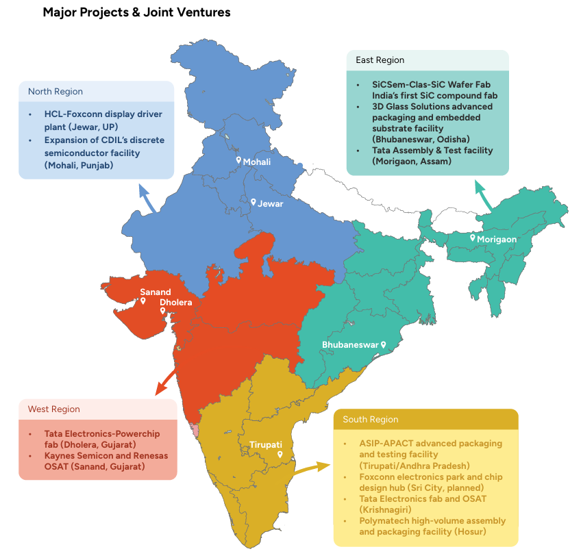
North India
North India is developing into a high-power discrete semiconductor ecosystem, with upcoming fabs focused on MOSFETs, IGBTs, and display driver ICs- all critical for consumer electronics, automotive, and power conversion applications. Mohali and Jewar are expected to be the region’s manufacturing anchor points in FY26–27.
| Category | Details |
| Key Nodes | Jewar (UP), Mohali (Punjab) |
| Anchor Companies | HCL, Foxconn, Continental Device India Ltd. (CDIL) |
| Flagship Projects | • HCL–Foxconn display driver fab (Jewar) • CDIL expansion for discrete devices (Mohali) |
| Primary Focus Areas | Display driver ICs, MOSFETs, IGBTs, packaging, testing |
South India
South India is rapidly becoming the largest semiconductor packaging and testing cluster in the country, driven by OSAT investments, mobility-focused chip development, and high-volume production capabilities. Tamil Nadu and Andhra Pradesh are leading the charge with multiple tier-1 facilities operational and expanding.
| Category | Details |
| Key Nodes | Tirupati (AP), Hosur (TN), Sri City (planned), Krishnagiri (TN) |
| Anchor Companies | ASIP Technologies (with APACT), Foxconn, Tata Electronics, Polymatech |
| Flagship Projects | • ASIP–APACT OSAT facility (Tirupati) • Foxconn chip design hub (Sri City) • Tata Electronics fab + OSAT (Krishnagiri) • Polymatech high-volume packaging (Hosur) |
| Primary Focus Areas | Advanced OSAT, ATMP, automotive & mobile chip packaging/testing |
West India
West India is the epicenter of front-end semiconductor manufacturing with the country’s largest fab infrastructure coming online in Gujarat. Dholera and Sanand are emerging as India’s answer to Taiwan’s Hsinchu and South Korea’s Pyeongtaek clusters, enabling true silicon-level fabrication.
| Category | Details |
| Key Nodes | Dholera, Sanand (Gujarat) |
| Anchor Companies | Tata Electronics, Renesas–CG Power, Kaynes Semicon |
| Flagship Projects | • Tata Electronics–Powerchip Wafer Fab (Dholera) • Kaynes Semicon + Renesas OSAT (Sanand) • Tata Semiconductor Assembly expansion |
| Primary Focus Areas | Wafer fabs, ATMP/OSAT, AI & automotive chips, silicon front-end manufacturing |
East India
East India stands out for deep-tech materials innovation, led by India’s first silicon carbide (SiC) compound fab- critical for EVs, aerospace, energy-efficient power electronics and high-temperature military applications. With 3D packaging capability added, it is set to become a next-gen manufacturing zone.
| Category | Details |
| Key Nodes | Bhubaneswar (Odisha), Morigaon (Assam) |
| Anchor Companies | SiCSem, 3D Glass Solutions, Tata Assembly & Test |
| Flagship Projects | • SiCSem + Clas-SiC India’s first SiC fab (Bhubaneswar) • 3D Glass Solutions packaging facility (Odisha) • Tata Assembly + Test expansion (Assam) |
| Primary Focus Areas | SiC chips for EV/defence, glass interposers, 3DHI, high-density substrates |
Key Challenges in Semiconductor Hiring
India’s semiconductor sector is scaling fast, but several structural and external challenges continue to shape hiring momentum. The India Decoding Jobs 2026 Report outlines the key hurdles and how they influence workforce demand:
| Challenge | Impact on Employment |
| Geopolitical uncertainties & supply chain risks | Semiconductor design GCCs recorded a 15% fall in active job openings in FY25, driven by global tensions and disrupted material flow. Continued constraints in supply chains and cross-border talent movement could further reduce advanced design and R&D roles through FY26–27. |
| Uncertain global tariff landscape | Volatile tariff policies add risk to export-linked chip production. Any withdrawal of semiconductor import exemptions could directly impact export-driven hiring pipelines, slowing recruitment for global projects. |
| Infrastructure gaps | Limited access to uninterrupted power, high-purity water, and clean-room facilities increases operational costs. These delays may push companies to stagger onboarding or reduce hiring speed for new fabs and OSAT units. |
| Beginner’s risk in first-gen fabs | Initial yield instability, process calibration, and quality ramp-up challenges may slow scaling. Early hires may require retraining, and full workforce absorption may take longer than projected. |
While the demand outlook for FY26–27 remains strong, hiring growth may not be uniform across regions or specialisations. Infrastructure readiness, policy stability, and manufacturing maturity will determine how fast the talent landscape scales.
Strengthening supply chain localisation, accelerating infrastructure upgrades, and de-risking early-stage fabs will be essential to sustain momentum and secure long-term job creation.
Global Semiconductor Trends
The global semiconductor industry recorded its highest-ever annual revenue in 2024- touching $627.6 billion, up 19.1% from 2023. Driven by demand for AI, high-performance computing, data centers, and memory, the market is projected to grow by another 11% in 2025, reaching nearly $697 billion.

Memory and logic segments dominated growth:
- Memory sales surged 78.9% to $165.1 billion
- Logic chips generated $212.6 billion
- AI accelerators and data-center silicon remain top drivers for 2026+ pipeline
However, rapid expansion has triggered a global talent shortage. The semiconductor workforce is expected to grow from 345,000 to 460,000 by 2030, but nearly 58% of new jobs, including 80% of technical roles may remain unfilled, largely due to low advanced-engineering graduation rates.
By 2029, McKinsey estimates that the industry will need:
| Role Category | Share of Global Workforce Gap |
| Engineering talent | 41% |
| Semiconductor technicians | 39% |
| Computer science & hardware roles | 20% |
Competition is intensifying for specialised skills in: advanced packaging, nano-fabrication, process engineering, chip design, EDA, photolithography, AI hardware & test automation.
Around 40% of semiconductor executives rank talent availability among their top three risks– alongside tariff volatility and trade restrictions. Capital investment remains strong, but workforce capacity is emerging as a limiting factor to growth.
Global hiring is already straining under talent shortfalls:
| Region | Estimated Workforce Gap |
| United States | 59,000–146,000 professionals by 2029 |
| Southeast Asia | 200,000 engineers required |
| Europe | 100,000+ openings in analog & mixed-signal |
| China | 300,000 professional shortfall |
| Taiwan | 34,000 vacancies, 80% rise in hiring demand |
China and Taiwan continue to lead advanced chipmaking but face acute shortages in R&D, fab engineers, and design experts, despite large-scale university programs and incentive schemes. Taiwan has begun exporting engineers overseas to support global fabs, adding pressure to domestic availability.
India’s Semiconductor Talent Landscape
India already represents 20% of the global semiconductor workforce, with hiring accelerating across design, fab, ATMP, and electronics manufacturing.
Workforce Scale & Expansion Outlook
- Semiconductor talent base expected to reach 2,20,000 professionals by FY2026
- Hiring pipeline aims to add 10 lakh jobs within the next 12 months
- Yet only a small fraction of 6 lakh electronics graduates yearly are job-ready for fabrication or VLSI roles
→ Skilling is the biggest unlock for growth
Hiring Hotspots
| Segment | Hiring Hubs |
| Chip design & R&D | Bengaluru, Hyderabad, Noida |
| Fab & ATMP expansion | Dholera, Greater Noida, Prayagraj, Mohali |
| Supply chain & manufacturing | Tamil Nadu, Gujarat, UP semiconductor corridors |
Salary Trends
Semiconductor professionals in India earn 25–35% more than mainstream IT roles, with top engineers earning up to ₹80 lakh annually. The strongest premiums are seen in roles involving:
- VLSI design
- AI silicon & accelerators
- Photolithography & process control
- Advanced OSAT/ATMP & packaging
Investment Momentum
India has already attracted ₹1.6 lakh crore in semiconductor investments, led by Tata Electronics, CG Power, Micron, Kaynes Semicon, HCL, SPEL Semiconductor, etc.
International players like AMD, Intel, Micron dominate high-complexity design, while Indian companies are building fab, ATMP & high-volume manufacturing capacity at scale.
National Skilling Push: Building an Industry-Ready Workforce
Government-led training initiatives are central to bridging India’s talent readiness gap.
Programs Driving Talent Development:
- Chips to Startup (C2S)
- ISM Semicon India Skill Platform
- AICTE VLSI Curriculum Upgrade
- SMART Lab (NIELIT Calicut) → 1,00,000 engineers targeted for training; 44,000 already trained
Despite progress, industry feedback indicates a continued shortfall in fab-ready, packaging-ready and test-engineering talent, underscoring the need for accelerated upskilling and academia-industry integration.
Get the full projections in Taggd’s India Decoding Jobs 2026 — Download the report for CHRO-grade insights.
Future Hiring Trends in Semiconductor Industry
India’s semiconductor industry is entering a high-growth hiring phase, backed by new fabs, ATMP facilities, design centers, and AI-integrated manufacturing.
Over the next two years, workforce demand will accelerate across fabrication, chip design, supply chain, and digital-engineering roles with the strongest traction in jobs that blend hardware engineering with AI-led automation and software capabilities.

Key Workforce Projections
- Of the 10 lakh semiconductor jobs expected by FY2026–27, nearly 3,00,000 roles will emerge in fabrication and another 2,00,000 in ATMP, forming the backbone of India’s next-gen silicon manufacturing ecosystem.
- The remaining job share will expand across chip design, VLSI, embedded systems, software development, supply-chain functions, QA/QC, materials engineering, procurement, and automation operations.
Infrastructure-Led Hiring Growth
The private sector will drive a majority of new workforce creation.
- Tata Electronics’ ₹91,000 crore fab in Dholera alone is expected to generate 20,000+ direct jobs, with long-tail employment in logistics, clean-room operations, and equipment maintenance.
- The HCL–Foxconn ₹3,706 crore ATMP unit in Jewar will further expand advanced manufacturing roles, helping establish North India as a semiconductor employment hub.
- Accelerated state approvals and investment incentives are triggering new semiconductor clusters in at least five additional industrial regions, opening opportunities for both fresh engineers and experienced lateral talent.
ATMP + Fabrication will account for nearly 50% of all new semiconductor jobs in India by FY27.
Rise of AI-Integrated and Digital-Skill Roles
Next-generation fabs and design units are ramping up hiring for:
- AI/ML engineers & data scientists
- Chip design & verification engineers (VLSI)
- Cybersecurity & systems reliability experts
- Digital twin, automation & predictive maintenance specialists
As manufacturing becomes AI-augmented and analytics-driven, talent with cross-disciplinary skill sets – hardware + software + automation will see the highest demand and salary growth.
Supply Chain Localisation = New Employment Scale
Domestic semiconductor production is projected to add 3,00,000+ roles in supply chain, materials management, procurement, and quality control by FY2026, strengthening India’s resilience against global trade and tariff shocks.
Wrapping Up
India’s semiconductor sector is entering its most critical growth phase yet. With fabs, ATMP units, design centres, and allied manufacturing ecosystems expanding at speed, the demand for skilled talent will accelerate across fabrication, packaging, chip design, AI engineering, and semiconductor supply chains.
If current investment momentum, skilling initiatives, and policy support continue, FY26–27 could mark the beginning of India’s rise as a global semiconductor talent powerhouse- generating employment at scale while advancing the nation’s digital and manufacturing capabilities.
FAQs
How many semiconductor jobs are expected by FY26–27?
India is projected to generate around 10 lakh semiconductor jobs by FY2026–27, driven by fabrication, ATMP expansion, chip design, and supply chain growth.
Which roles will see the highest hiring demand?
Fabrication and ATMP are expected to account for nearly 50% of openings, followed by chip design, materials engineering, data science, AI/ML, and supply chain jobs.
Which companies are leading semiconductor hiring in India?
Key hiring drivers include Tata Electronics (Dholera fab), HCL–Foxconn (Jewar ATMP), along with several upcoming fabrication and ATMP clusters supported by state incentives.
Will AI and automation reduce job opportunities?
No. AI adoption is increasing demand for digital-skilled roles like chip designers, cybersecurity experts, data scientists, and predictive maintenance engineers.
What skills are most in demand for semiconductor careers?
VLSI, process engineering, advanced materials, cleanroom operations, embedded systems, AI, digital twins, and semiconductor equipment handling are top skill priorities.
Are there opportunities for freshers?
Yes, especially in ATMP, fabrication operations, testing, supply chain support, and technician-level roles- provided candidates have relevant technical training.
What does the talent landscape look like by FY2027?
If investment and skilling pipelines continue, India could become one of the world’s fastest-expanding semiconductor workforces, with a strong tilt toward advanced technical and digital jobs.
To get deeper insights into Semiconductor hiring trends, AI-based workforce transformation, and India’s talent demand outlook, download the full India Decoding Jobs 2026 report- complete data, hiring charts, industry forecasts & strategic recommendations.
Download Now- India Decoding Jobs 2026. Explore Taggd for RPO solutions.